

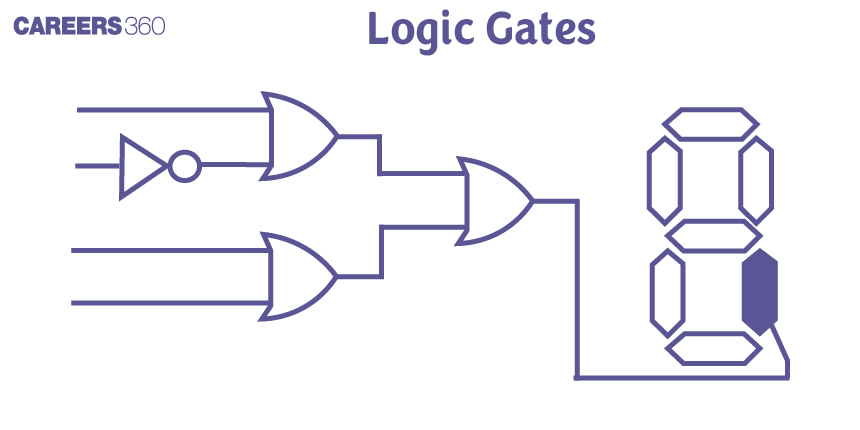
Logic Gates
Logic gates are the fundamental building blocks of digital circuits. They perform basic logical functions that are essential for digital computation. Each gate operates on one or more binary inputs to produce a single binary output. The most common types of logic gates are AND, OR, NOT, NAND, NOR, XOR, and XNOR. These gates are used extensively in various electronic devices, from simple calculators to complex computer systems, enabling them to perform a wide range of operations.
This Story also Contains
- Logic Gates
- D'morgan's Theorem
- Solved Example Based On Logic Gates
- Summary
Logic gates can be found in many everyday devices. For instance, an automatic lighting system in a room can use an AND gate to turn on the light only when both conditions are met: it's dark outside (sensor input) and someone is in the room (motion detector input). Similarly, a security alarm system might use an OR gate to sound the alarm if any one of several conditions is true, such as a door or window being opened. Let's discuss the logic gates and important relations to solve complex problems related to gates.
Logic Gates
In our day-to-day life, we come across many digital electronic devices. But do you know, for digital devices to function the way they do, a logic needs to be established between the input and output voltages. This is done by using a gate or a digital circuit that follows the logical relationship. They are called logic gates because they control the flow of information based on a certain logic.
Symbols are given to each logic gate and each logic gate has a truth table which displays all possible input-output combinations. So the truth tables help understand the behaviour of the logic gates. All these gates are made using semiconductor devices. The five most commonly used logic gates are:
- NOT
- AND
- OR
- NAND
- NOR
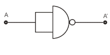
NOT Gate
A NOT gate is also known as an inverter because it simply inverts the input signal. It is a simple gate with one input and one output. So, the output is ‘0’ when the input is ‘1’ and vice-versa.
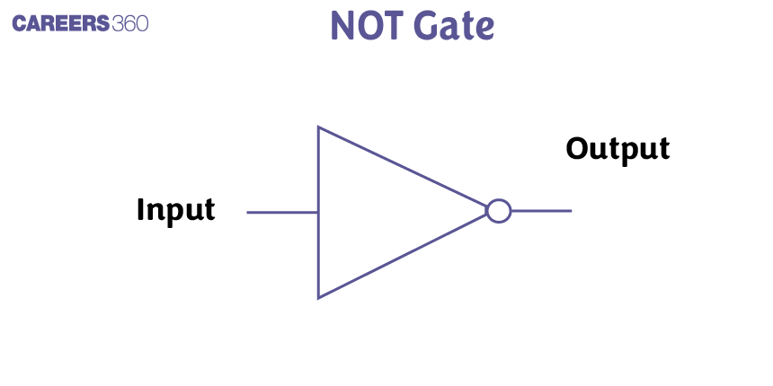
A is input
Y is output
$Y=\bar{A}$
The truth table for a NOT gate is as follows:
.png)
AND Gate
An AND gate has two or more inputs and a single output. In this gate, the output is 1(High) only when all the inputs are 1(High). The most commonly used symbol for an AND gate is as follows:
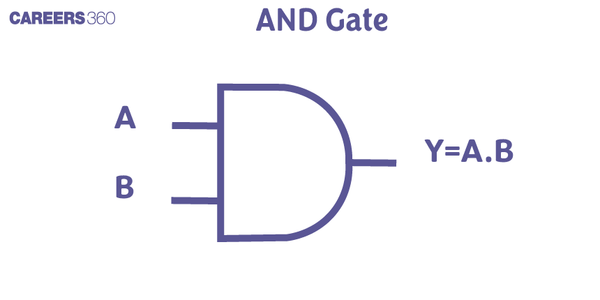
$A$ and $B$ are input
Y is output
$
Y=A \cdot B
$
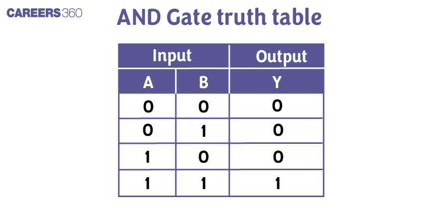
The truth table for the AND gate is as follows
OR Gate
Like AND Gate, OR gate has also two or more inputs and one output. For this Gate, the logic is that the output would be 1 when at least one of the inputs is 1. It means when the output is high when any of the input is high. The commonly used symbol for an OR gate is as follows:
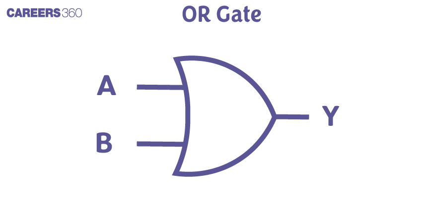
$A$ and $B$ are input
Y is output
Relation between input and output
$
Y=A+B
$
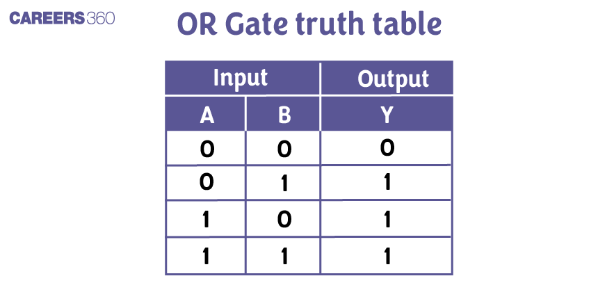
And, the truth table for an OR gate is as follows:
![OR%20Gate%20Truth%20Table]() NAND Gate
NAND Gate
A NAND gate is an arrangement of an AND gate followed by a NOT gate. The output is 1 only when all inputs are NOT 1 Or the output is high when at least one of them is low. These are also called Universal gates. The commonly used symbol for a NAND gate is as follows:
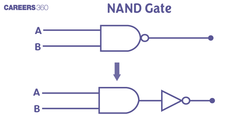
$
Y=\overline{A \cdot B}
$
$A$ and $B$ are input
Y is output
NOT + AND gate
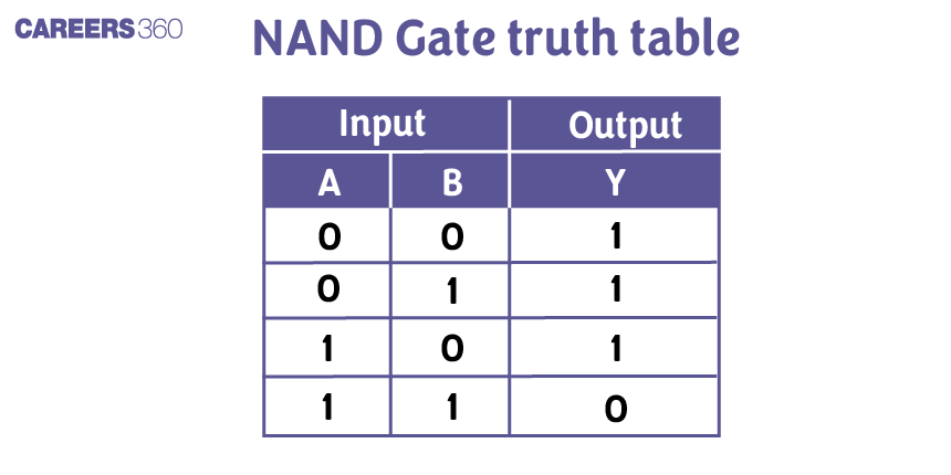
And, the truth table for a NAND gate is as follows:
NOR Gate
Like the NAND Gate, the NOR gate is also an arrangement of an OR gate followed by a NOT gate. In this, the output is 1(High) only when all inputs are 0(Low). These are also called Universal gates. The commonly used symbol for a NOR gate is as follows:
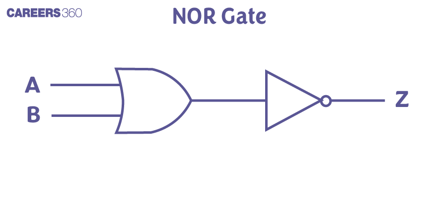 $
$
Y=\overline{A+B}
$
$A$ and $B$ are input
Y is output
NOT + OR Gate
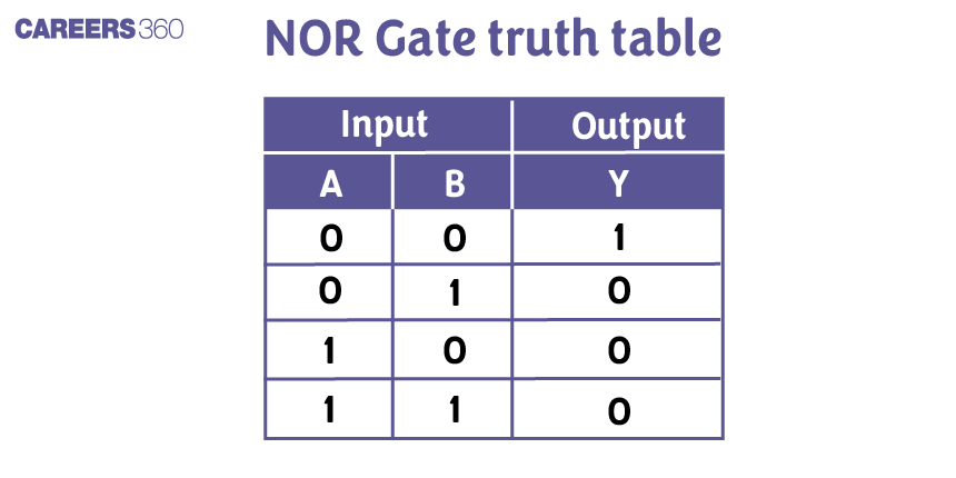
The truth table for a NOR gate is as follows:
![NOR%20Gate%20truth%20table]() D'morgan's Theorem
D'morgan's Theorem
De Morgan's Theorems are used to simplify complex Boolean expressions, which is essential for designing and optimizing digital circuits. These theorems are fundamental rules in Boolean algebra that describe the relationship between the logical operators AND, OR, and NOT.
if $A$ and $B$ are input then
1) $\overline{A+B}=\bar{A} \cdot \bar{B}$
2) $\overline{A \cdot B}=\bar{A}+\bar{B}$
3) $\overline{A+\bar{B}}=A \cdot B$
4) $\overline{A \cdot \bar{B}}=A+B$
Some Important relations
$
\begin{aligned}
& A+A=A \\
& A \cdot A=A \\
& A+1=1 \\
& A \cdot 1=1 \\
& A \cdot 0=0 \\
& A+0=A
\end{aligned}
$
Recommended Topic Video
Solved Example Based On Logic Gates
Example 1: Boolean relation at the output stage - Y for the following circuit is :

1) $\bar{A}+\bar{B}$
2) $A+B$
3) $A B$
4) $\bar{A} \cdot \bar{B}$
Solution:
The first part of the given circuit represents or gate whose output is A+B
The second part of the circuit is NOT a gate whose input is A+B and whose output is $\overline{A+B}=\bar{A} \cdot \bar{B}$
Hence, the answer is option (4).
Example 2: A system of four gates is set up as shown. The ' truth table ' corresponding to this system is :

1)
2)
3)
4)
Solution:
In the given system all four gates are NOR gates.
$\begin{array}{|c|c|c|c|c|c|} \hline \mathrm{A} & \mathrm{B} & \left(\mathrm{y}^{\prime}=\overline{\mathrm{A}+\mathrm{B}}\right) & \mathrm{y}^{\prime \prime}=(\overline{\mathrm{A}+\mathrm{y}^{\prime}}) & \mathrm{y}^{\prime \prime \prime}=(\overline{\mathrm{B}+\mathrm{y}^{\prime}}) & \mathrm{y}=\overline{\mathrm{y}^{\prime \prime}+\mathrm{y}^{\prime \prime \prime}} \\ \hline 0 & 0 & 1 & 0 & 0 & 1 \\ \hline 0 & 1 & 0 & 1 & 0 & 0 \\ \hline 1 & 0 & 0 & 0 & 1 & 0 \\ \hline 1 & 1 & 0 & 0 & 0 & 1 \\ \hline \end{array}$
i.e
$\begin{array}{|c|c|c|} \hline \mathrm{A} & \mathrm{B} & \mathrm{y} \\ \hline 0 & 0 & 1 \\ \hline 0 & 1 & 0 \\ \hline 1 & 0 & 0 \\ \hline 1 & 1 & 1 \\ \hline \end{array}$
Example 3: Which of the following gives a reversible operation?
1)
2) 
3)
4)
Solution:
For reversible operation, NOT gate is used. If an input isthen output=
. The following circuit represents the NOT gate
Example 4: Which of the following circuits correctly represents the following truth table?

1) 
2)
3)
4)
Solution:
For circuit 1 ,
$
A \cdot B=\overline{Y+\bar{A}}=C
$
and the truth table for circuit 1 matches the truth table given in the question
Example 5: Identify the operation performed by the circuit given below:

1) NAND
2) OR
3) AND
4) NOT
Solution:

Behaves like a not gate so Boolean equation will be
$
\begin{aligned}
y & =\overline{A+B+C} \\
y & =A \cdot B \cdot C
\end{aligned}
$
whole arrangement behaves like an AND gate
Summary
Logic gates, such as AND, OR, NOT, NAND, and NOR, are the fundamental building blocks of digital circuits, performing essential logical functions. Each gate operates on one or more binary inputs to produce a single binary output. These gates are crucial for designing and operating various electronic devices, enabling them to perform a wide range of operations. Symbols and truth tables help in understanding their behaviour, making it easier to design and analyze digital circuits.
