

Common Emitter (NPN/PNP) Transistor: Characteristics and Gains
The common emitter (CE) transistor configuration is a fundamental circuit used extensively in electronics, particularly for amplifying signals. In a CE configuration, either an NPN or PNP transistor is used, with the emitter terminal common to both the input and output circuits. This setup allows for significant amplification of the input signal, making it ideal for use in various electronic devices, from radios to amplifiers. The behaviour of the transistor in this configuration is governed by the relationship between the base current (IB), collector current (IC), and the voltage across the collector-emitter junction (VCE). Key characteristics, such as the input and output characteristics, help determine the current gain (β) and the voltage gain, which are crucial parameters for designing circuits. By analyzing these characteristics, one can understand the transistor's response to different inputs and how effectively it can amplify signals.
This Story also Contains
- Aim
- Apparatus
- Theory
- Formula Used
- Diagram
- Procedure
- For Input Characteristics
- Observations
- Calculations
- Some Solved Examples
- Summary
Aim
To study the characteristics of a common emitter npn (or pnp) transistor and to find out the values of current and voltage gains.
Apparatus
An n-p-n transistor, a three-volt battery, a 30-volt battery, two high resistance rheostats, one 0-3 volt voltmeter, one 0-30 volt voltmeter, one 0-50 micro-ammeter, one 0 - 50 mA milli-ammeter, two one way keys, connecting wires.
Theory
In the common-emitter circuit of a transistor, the emitter-base makes the input section and the emitter-collector makes the output section. As usual, the base junction (input junction) is forward and collector junction (output
junction) is reverse-biased.
The resistance offered by the base junction is called input resistance (R) It has a very small resistance due to forward biasing.
The resistance offered by the collector junction is called output resistance (R0). \text { It has a high value due to reverse } biasing.
Due to high output resistance (resistance in the output section), high resistance can be used as load resistance (RL ).Generally $R_L=R_0$
The ratio $\frac{R_L}{R_I}=\frac{R_0}{R_I}$ measures the resistance gain of the common emitter transistor. It is of the order of one thousand. The current equation,$I_e=I_b+I_c$
Also emitter current ( $\left(l_e\right.$ ) divides itself into base current $\left(l_b\right)$ and collector current $\left(l_c\right)$. In the $n-p-n$ transistor, $\mathrm{I}_{\mathrm{c}}$ is about $98 \%$ of $\mathrm{I}_{\mathrm{e}}$, the base current $\mathrm{I}_{\mathrm{b}}$ remains only $2 \%$ of $\mathrm{l}_{\mathrm{e}}$. A Little change in $\mathrm{l}_{\mathrm{b}}$ causes a large change (about 49 times) in $l_c$. The ratio of change in collector current to the corresponding change in base current, which measures current gain in the common emitter transistor. It is represented by the symbol $\beta$.
$\beta=\frac{\Delta I_c}{\Delta I_b}$
Formula Used
Input resistance, $R_I=\frac{\Delta V_b}{\Delta I_b}$
Output resistance, $R_o=\frac{\Delta V_c}{\Delta I_c}$
Resistance gain $=\frac{R_0}{R_I}$
Current gain, $\beta=\frac{\Delta I_c}{\Delta I_b}$
Voltage gain $=$ Current gain $\times$ Resistance gain
$
A_V=\beta \cdot \frac{R_0}{R_I}
$
Diagram
![]()
Procedure
1. Make a circuit diagram as shown in the figure.
2. Make all connections neat, clean and tight.
3. Note least count and zero errors of voltmeters and ammeters.
4. Make voltmeter readings zero in V1 and V2 and insert the keys.
For Input Characteristics
5. Apply forward bias voltage on the base junction. Read base voltage $\mathrm{V}_{\mathrm{b}}$ and base current $\mathrm{I}_{\mathrm{b}}$.
6. Go on increasing $\mathrm{V}_{\mathrm{b}}$ till $l_{\mathrm{b}}$ rises suddenly. Note corresponding values of $l_{\mathrm{b}}$ for each value of $\mathrm{V}_{\mathrm{b}}$.
7. Make collector voltage $\mathrm{V}_{\mathrm{C}}=10 \mathrm{~V}$ and repeat steps 5 and 6 .
8. Repeat step 7 with $\mathrm{V}_{\mathrm{C}}=20 \mathrm{~V}$ and 30 V .
9. Make all readings zero.
For output characteristics
10. Keep collector voltage $\left(\mathrm{V}_{\mathrm{c}}\right)$ zero. Adjust base voltage $\mathrm{V}_{\mathrm{b}}$ to make base current $\mathrm{l}_{\mathrm{b}}=10 \mu \mathrm{A}$. Though collector voltage $\mathrm{V}_{\mathrm{c}}$ is zero; but there is collector current $\mathrm{I}_{\mathrm{c}}\{\mathrm{Note}$ it. $\}$
11. Make collector voltage $10 \mathrm{~V}, 20 \mathrm{~V}$ and 30 V and note the corresponding collector currents.
12. Repeat steps 10 and 11 with $\mathrm{l}_{\mathrm{b}}=20 \mu \mathrm{A}, 30 \mu \mathrm{A}$, and $40 \mu \mathrm{A}$.
13. Record your observations as given below:
Observations
Least count of voltmeter, $\mathrm{V}_1=\ldots . . \mathrm{V}$
Zero error of voltmeter, $\quad \mathrm{V}_1=\ldots . . \mathrm{V}$
Least count of voltmeter, $\quad \mathrm{V}_2=\ldots . . \mathrm{V}$
Zero error of voltmeter, $\quad \mathrm{V}_2=\ldots . \mathrm{V}$
Least count of milli-ammeter $=\ldots \ldots \mathrm{mA}$
Zero error of milli-ammeter $\quad=\ldots \mathrm{mA}$
Least count of micro-ammeter $=\ldots \ldots . \mu \mathrm{A}$
Zero error of micro-ammeter $\quad=\ldots \ldots . \mu \mathrm{A}$
Calculations
1. Calculation for input resistance (RI)
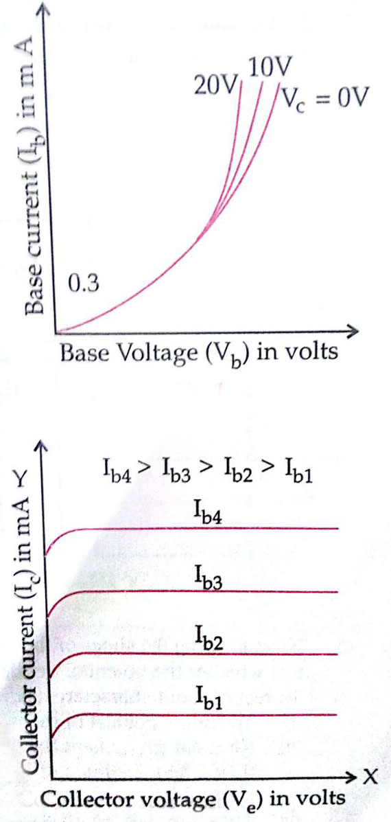
Plot a graph between base voltage Vb and base current lb for zero collector voltage Vc, taking Vb along X-axis and lb along the Y-axis. Plot graphs for different values of Vc. The graphs come as shown. These graphs are called the 'input characteristics' of the transistor.
The slope of the graphs becomes large at the ends. The slope gives value of $\frac{\Delta I_b}{\Delta V_b}$. Its reciprocal $\frac{\Delta V_b}{\Delta I_b}$ gives input resistance $\mathrm{R}_1$. As graphs run parallel near the ends, all give the same value of $\mathrm{R}_1$.
![]()
2. Calculation for output resistance $\left(\mathrm{R}_0\right)$
Plot a graph between collector voltage $\mathrm{V}_{\mathrm{c}}$ and collector current $\mathrm{I}_{\mathrm{c}}$ for $10 \mu \mathrm{A}$ base current $\mathrm{l}_{\mathrm{b}}$, taking $\mathrm{V}_{\mathrm{c}}$ along X -axis and $I_{\mathrm{c}}$ along Y -axis. Plot graphs for different values of $\mathrm{l}_{\mathrm{b}}$.
![]()
These graphs are called the 'output characteristics' of the transistor.
The slope of the graphs becomes almost zero at the ends. The slope gives value of $\frac{\Delta I_e}{\Delta V_e}$. Its reciprocal $\frac{\Delta V_e}{\Delta I_e}$ gives output resistance $\mathrm{R}_0$. As graphs run parallel near the ends, all give the same values of $\mathrm{R}_0$.
3. Calculation for current gain $(\beta)$
Plot a graph between base current $\mathrm{I}_b$ ) and corresponding collector current $\mathrm{I}_{\mathrm{c}}$ ( for 30 volts collector voltage ) $\mathrm{V}_{\mathrm{c}}$, taking $\mathrm{l}_{\mathrm{b}}$ along X -axis and $\mathrm{l}_{\mathrm{c}}$ along Y -axis. The graph comes to be a straight line. The graph is called current gain characteristic of the common emitter transistor.
The slope of the straight line gives value of $\frac{\Delta I_c}{\Delta I_b}$ which is the value of current gain $\beta$ of the common emitter transistor.
![]()
4. Calculation for voltage gain $\mathrm{A}_{\mathrm{V}}$
From relation, Voltage gain $=$ Current gain $\times$ Resistance gain
$
A_v=\beta \times \frac{R_0}{R_I}
$
Result
For the given common emitter transistor,
Current gain, $\beta=\ldots$.
Voltage gain, $\quad A_v=\ldots \ldots$
Some Solved Examples
Example 1: Why a common emitter transistor is preferred over a common base transistor?
1) Because the thickness of the emitter section is much larger than that of the base section.
2) Because the current gain in CB mode is much larger than that in CE mode
3) Because the current gain in CE mode is much larger than that in CB mode.
4) Because of the infinite input resistance of the common Base transistor.
Solution
To study the characteristics of common emitter n-p-n or p-n-p transistor
$\begin{aligned} & \text { Input characters. } \\ & \mathrm{r}_{\mathrm{i}=}\left[\frac{\Delta V_{B E}}{\Delta I_B}\right]_{V_{C E}}=\text { Const. } \\ & \mathrm{ri}=\text { Input resistance } \\ & \mathrm{r}_{\mathrm{o}}=\text { Output resistance }= \\ & \Delta \mathrm{V}_{\mathrm{BE}}=\text { Base-Emitter Voltage } \\ & \Delta \mathrm{I}_{\mathrm{B}}=\text { Change in base current } \\ & \qquad\left[\frac{\Delta V_{C E}}{\Delta I_C}\right]_{I_B}=\text { Const. } \\ & \mathrm{ro}=\left[V_{C E}=\text { Change in collector-emitter voltage }\right. \\ & \Delta I_C=\text { Change in collector current }\end{aligned}$
wherein
If the graph is plotted between IB (base current) and VBE = Voltage of base - Emitter then it shows input character.
If the graph is plotted between Ic and Vce keeping base (IB) const. it is known as output characteristics
Example 2: In a similar base configuration, the current emitter changes by 2 mA when the emitter voltage is changed to 200 mA at a fixed collector to base voltage. the input resistance is
1) $100 \Omega$
2) $1000 \Omega$
3) $2.5 \Omega$
4) $4 \Omega$
Solution :
Given that:
$
\begin{aligned}
& V=200 \mathrm{mV}=200 \times 10^{-3} \mathrm{~V} \\
& I=2 \mathrm{~mA}=2 \times 10^{-3} \mathrm{~A}
\end{aligned}
$
The dynamic resistance is the ratio of the change in emitter voltage to the change in emitter current.
$
\begin{aligned}
& r_d=\frac{\Delta V}{\Delta I} \\
& r_d=\frac{200 \times 10^{-3}}{2 \times 10^{-3}}=100 \Omega
\end{aligned}
$
Hence the answer is Option (1).
Example 3: In a transistor, the current amplification factor is 0.6. A transistor is connected in the same emitter configuration, the change in collector current is when the base current changes by 6mA.
1) 6mA
2) 4.8mA
3) 24mA
4) 9mA
Solution:
Given that,
$
\begin{aligned}
& \alpha=0.8 \\
& I_b=6 \mathrm{~mA} \\
& \beta=\frac{\alpha}{1-\alpha}=\frac{0.6}{1-0.6}=\frac{0.6}{0.4}=\frac{3}{2}=1.5
\end{aligned}
$
Since,
$
\begin{aligned}
& \beta=\frac{I_c}{I_b} \\
& \Rightarrow I_c=\beta I_b \\
& I_c=(1.5)(6)=9 \mathrm{~mA}
\end{aligned}
$
Hence, the answer is the option (4).
Example 4: For the transistor, the value of α is 0.8. The change in the collector current corresponding to a change of 4mA in the base current in a common base arrangement is:
1) 16mA
2)72mA
3)18mA
4)54mA
Solution:
$\begin{aligned} & \therefore 0.8=\alpha \\ & \alpha=0.8=\frac{I_c}{I_\epsilon}=\frac{I_c}{\Delta I_c+\Delta I_B} \\ & 0.8\left(\Delta I_c+4\right)=\Delta I_c \\ & 0.8 \Delta I_c+3.2=\Delta I_c \\ & 0.2 \Delta I_c=3.2 \\ & \Delta I_c=\frac{3.2}{0.2}=16 \mathrm{~mA}\end{aligned}$
Hence, the answer is the option (1).
Summary
In a common emitter transistor experiment, the focus is on studying the input and output characteristics to determine the current and voltage gains. The input characteristics are obtained by varying the base-emitter voltage (VBE) and measuring the corresponding base current (IB) while keeping the collector-emitter voltage (VCE) constant. The output characteristics are observed by varying VCE and measuring the collector current (IC) for different values of IB. From these measurements, the current gain (β = IC / IB) and voltage gain can be calculated. The experiment demonstrates the transistor's ability to amplify current and voltage, confirming its utility in amplification applications. Understanding these characteristics is essential for designing and optimizing electronic circuits, especially in applications where signal amplification is required.
